
 Download Sample


Author
Prem Kumar with profound experience and sound knowledge across a wide range of market forecasting methods, demand f.....
Thin Film Encapsulation Market: By Application, By End-User, By Technology, and Region Forecast 2021-2032
Report ID:40883
Published Date:Sep 2025
No of Pages:236
Format:

Thin Film Encapsulation Market size was valued at US$ 308.3 million in 2025 and is expected to reach US$ 1,023.6 million by 2032, growing at a significant CAGR of 18.7% from 2026-2032. Demand for microelectronics and consumer electronics products drives the market. The evolution of microelectronics technology, a wide range of applications for various products in the electronics industry, and applications to other sectors are expected to fuel the market. The major changes include a higher level of product integration, better product performance, reliability, and reduced costs expected to drive microelectronics demand.
The encapsulation enables the expansion of the lifetime considerably. Good encapsulation relies on good-quality thin films. Widely used deposition methods are PECVD, atomic layer deposition (ALD), and parylene deposition. During the projection period, demand for semiconductor ICs is likely to be fueled by an increase in microelectronics and consumer electronics sales. The rising need for semiconductor integrated circuits is expected to boost semiconductor device manufacturers' production capacity, which could boost market demand. In 2022, the microsystems segment accounted for a larger revenue share and was projected to grow with a CAGR of 19.2% from 2023 to 2029 to reach US$ 254.3 mn by 2029.
Study Period
2026-2032Base Year
2025CAGR
18.7%Largest Market
Asia-PacificFastest Growing Market
North-America
The market has been propelled by an increase in the need for thin-film barriers in various flexible devices, a surge in the adoption rate of flexible OLED displays for smart devices, and increased capital investments in OLED technology. On the other side, a lack of technological understanding and the spread of flexible glass technology could hinder the global industry.
Due to the availability of several manufacturers of brands and various display panels in Japan, China, Hong Kong, South Korea, and Taiwan, APAC accounted for the largest revenue share in the global thin-film encapsulation market in 2021, with USD 116.8 Mn, and is expected to grow at a significant CAGR over the forecast years. The development of the regional market can also be linked to the advancement of the electronics and semiconductor sectors, particularly in China.
North America accounted for a significant revenue share in the global thin-film encapsulation market over the forecast years, owing to the presence of solar cell developers.
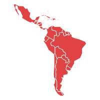
Latin America
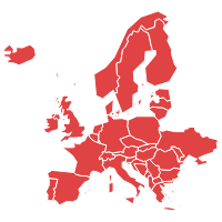
Europe
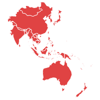
Asia Pacific
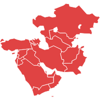
Middle East
North America
|
Report Benchmarks |
Details |
|
Report Study Period |
2026-2032 |
|
Market CAGR |
18.7% |
|
By Application |
|
|
By Technology |
|
|
By End User |
|
|
By Region |
|
Download Free Sample Report
![]()
The thin film encapsulation market size was valued at US$ 308.3 million in 2025 and is expected to reach US$ 1,023.6 million by 2032, growing at a significant CAGR of 18.7% from 2026-2032.
The key players of the market are Samsung SDI, LG Chem, Universal Display Corp., Applied Materials, Veeco Instruments
North America is the fastest-growing region for the market.
Content Updated Date: Feb 2026
| 1.Executive Summary |
| 2.Global Thin Film Encapsulation Market Introduction |
| 2.1.Global Thin Film Encapsulation Market - Taxonomy |
| 2.2.Global Thin Film Encapsulation Market - Definitions |
| 2.2.1.Application |
| 2.2.2.Technology |
| 2.2.3.End User |
| 2.2.4.Region |
| 3.Global Thin Film Encapsulation Market Dynamics |
| 3.1. Drivers |
| 3.2. Restraints |
| 3.3. Opportunities/Unmet Needs of the Market |
| 3.4. Trends |
| 3.5. Product Landscape |
| 3.6. New Product Launches |
| 3.7. Impact of COVID 19 on Market |
| 4.Global Thin Film Encapsulation Market Analysis, 2021 - 2025 and Forecast 2026 - 2032 |
| 4.1. Market Analysis, 2021 - 2025 and Forecast 2026 - 2032, (Sales Value USD Million) |
| 4.2. Year-Over-Year (Y-o-Y) Growth Analysis (%) |
| 4.3. Market Opportunity Analysis |
| 5.Global Thin Film Encapsulation Market By Application, 2021 - 2025 and Forecast 2026 - 2032 (Sales Value USD Million) |
| 5.1. Printed Circuit Board |
| 5.1.1. Market Analysis, 2021 - 2025 and Forecast 2026 - 2032, (Sales Value USD Million) |
| 5.1.2. Year-Over-Year (Y-o-Y) Growth Analysis (%) and Market Share Analysis (%) |
| 5.1.3. Market Opportunity Analysis |
| 5.2. Sensors |
| 5.2.1. Market Analysis, 2021 - 2025 and Forecast 2026 - 2032, (Sales Value USD Million) |
| 5.2.2. Year-Over-Year (Y-o-Y) Growth Analysis (%) and Market Share Analysis (%) |
| 5.2.3. Market Opportunity Analysis |
| 5.3. Microsystems |
| 5.3.1. Market Analysis, 2021 - 2025 and Forecast 2026 - 2032, (Sales Value USD Million) |
| 5.3.2. Year-Over-Year (Y-o-Y) Growth Analysis (%) and Market Share Analysis (%) |
| 5.3.3. Market Opportunity Analysis |
| 6.Global Thin Film Encapsulation Market By Technology, 2021 - 2025 and Forecast 2026 - 2032 (Sales Value USD Million) |
| 6.1. PECVD |
| 6.1.1. Market Analysis, 2021 - 2025 and Forecast 2026 - 2032, (Sales Value USD Million) |
| 6.1.2. Year-Over-Year (Y-o-Y) Growth Analysis (%) and Market Share Analysis (%) |
| 6.1.3. Market Opportunity Analysis |
| 6.2. ALD |
| 6.2.1. Market Analysis, 2021 - 2025 and Forecast 2026 - 2032, (Sales Value USD Million) |
| 6.2.2. Year-Over-Year (Y-o-Y) Growth Analysis (%) and Market Share Analysis (%) |
| 6.2.3. Market Opportunity Analysis |
| 6.3. Inkjet Printing |
| 6.3.1. Market Analysis, 2021 - 2025 and Forecast 2026 - 2032, (Sales Value USD Million) |
| 6.3.2. Year-Over-Year (Y-o-Y) Growth Analysis (%) and Market Share Analysis (%) |
| 6.3.3. Market Opportunity Analysis |
| 6.4. VTE |
| 6.4.1. Market Analysis, 2021 - 2025 and Forecast 2026 - 2032, (Sales Value USD Million) |
| 6.4.2. Year-Over-Year (Y-o-Y) Growth Analysis (%) and Market Share Analysis (%) |
| 6.4.3. Market Opportunity Analysis |
| 6.5. Others |
| 6.5.1. Market Analysis, 2021 - 2025 and Forecast 2026 - 2032, (Sales Value USD Million) |
| 6.5.2. Year-Over-Year (Y-o-Y) Growth Analysis (%) and Market Share Analysis (%) |
| 6.5.3. Market Opportunity Analysis |
| 7.Global Thin Film Encapsulation Market By End User, 2021 - 2025 and Forecast 2026 - 2032 (Sales Value USD Million) |
| 7.1. Medical Device Manufacturers |
| 7.1.1. Market Analysis, 2021 - 2025 and Forecast 2026 - 2032, (Sales Value USD Million) |
| 7.1.2. Year-Over-Year (Y-o-Y) Growth Analysis (%) and Market Share Analysis (%) |
| 7.1.3. Market Opportunity Analysis |
| 7.2. Aerospace |
| 7.2.1. Market Analysis, 2021 - 2025 and Forecast 2026 - 2032, (Sales Value USD Million) |
| 7.2.2. Year-Over-Year (Y-o-Y) Growth Analysis (%) and Market Share Analysis (%) |
| 7.2.3. Market Opportunity Analysis |
| 7.3. Electrical Cars |
| 7.3.1. Market Analysis, 2021 - 2025 and Forecast 2026 - 2032, (Sales Value USD Million) |
| 7.3.2. Year-Over-Year (Y-o-Y) Growth Analysis (%) and Market Share Analysis (%) |
| 7.3.3. Market Opportunity Analysis |
| 7.4. Others |
| 7.4.1. Market Analysis, 2021 - 2025 and Forecast 2026 - 2032, (Sales Value USD Million) |
| 7.4.2. Year-Over-Year (Y-o-Y) Growth Analysis (%) and Market Share Analysis (%) |
| 7.4.3. Market Opportunity Analysis |
| 8.Global Thin Film Encapsulation Market By Region, 2021 - 2025 and Forecast 2026 - 2032 (Sales Value USD Million) |
| 8.1. North America |
| 8.1.1. Market Analysis, 2021 - 2025 and Forecast 2026 - 2032, (Sales Value USD Million) |
| 8.1.2. Year-Over-Year (Y-o-Y) Growth Analysis (%) and Market Share Analysis (%) |
| 8.1.3. Market Opportunity Analysis |
| 8.2. Europe |
| 8.2.1. Market Analysis, 2021 - 2025 and Forecast 2026 - 2032, (Sales Value USD Million) |
| 8.2.2. Year-Over-Year (Y-o-Y) Growth Analysis (%) and Market Share Analysis (%) |
| 8.2.3. Market Opportunity Analysis |
| 8.3. Asia Pacific (APAC) |
| 8.3.1. Market Analysis, 2021 - 2025 and Forecast 2026 - 2032, (Sales Value USD Million) |
| 8.3.2. Year-Over-Year (Y-o-Y) Growth Analysis (%) and Market Share Analysis (%) |
| 8.3.3. Market Opportunity Analysis |
| 8.4. Middle East and Africa (MEA) |
| 8.4.1. Market Analysis, 2021 - 2025 and Forecast 2026 - 2032, (Sales Value USD Million) |
| 8.4.2. Year-Over-Year (Y-o-Y) Growth Analysis (%) and Market Share Analysis (%) |
| 8.4.3. Market Opportunity Analysis |
| 8.5. Latin America |
| 8.5.1. Market Analysis, 2021 - 2025 and Forecast 2026 - 2032, (Sales Value USD Million) |
| 8.5.2. Year-Over-Year (Y-o-Y) Growth Analysis (%) and Market Share Analysis (%) |
| 8.5.3. Market Opportunity Analysis |
| 9.North America Thin Film Encapsulation Market ,2021 - 2025 and Forecast 2026 - 2032 (Sales Value USD Million) |
| 9.1. Application Analysis 2021 - 2025 and Forecast 2026 - 2032 by Sales Value USD Million, Y-o-Y Growth (%), and Market Share (%) |
| 9.1.1.Printed Circuit Board |
| 9.1.2.Sensors |
| 9.1.3.Microsystems |
| 9.2. Technology Analysis 2021 - 2025 and Forecast 2026 - 2032 by Sales Value USD Million, Y-o-Y Growth (%), and Market Share (%) |
| 9.2.1.PECVD |
| 9.2.2.ALD |
| 9.2.3.Inkjet Printing |
| 9.2.4.VTE |
| 9.2.5.Others |
| 9.3. End User Analysis 2021 - 2025 and Forecast 2026 - 2032 by Sales Value USD Million, Y-o-Y Growth (%), and Market Share (%) |
| 9.3.1.Medical Device Manufacturers |
| 9.3.2.Aerospace |
| 9.3.3.Electrical Cars |
| 9.3.4.Others |
| 9.4. Country Analysis 2021 - 2025 and Forecast 2026 - 2032 by Sales Value USD Million, Y-o-Y Growth (%), and Market Share (%) |
| 9.4.1.United States of America (USA) |
| 9.4.2.Canada |
| 10.Europe Thin Film Encapsulation Market ,2021 - 2025 and Forecast 2026 - 2032 (Sales Value USD Million) |
| 10.1. Application Analysis and Forecast by Sales Value USD Million, Y-o-Y Growth (%), and Market Share (%) |
| 10.1.1.Printed Circuit Board |
| 10.1.2.Sensors |
| 10.1.3.Microsystems |
| 10.2. Technology Analysis 2021 - 2025 and Forecast 2026 - 2032 by Sales Value USD Million, Y-o-Y Growth (%), and Market Share (%) |
| 10.2.1.PECVD |
| 10.2.2.ALD |
| 10.2.3.Inkjet Printing |
| 10.2.4.VTE |
| 10.2.5.Others |
| 10.3. End User Analysis 2021 - 2025 and Forecast 2026 - 2032 by Sales Value USD Million, Y-o-Y Growth (%), and Market Share (%) |
| 10.3.1.Medical Device Manufacturers |
| 10.3.2.Aerospace |
| 10.3.3.Electrical Cars |
| 10.3.4.Others |
| 10.4. Country Analysis 2021 - 2025 and Forecast 2026 - 2032 by Sales Value USD Million, Y-o-Y Growth (%), and Market Share (%) |
| 10.4.1.Germany |
| 10.4.2.France |
| 10.4.3.Italy |
| 10.4.4.United Kingdom (UK) |
| 10.4.5.Spain |
| 10.4.6.Rest of EU |
| 11.Asia Pacific (APAC) Thin Film Encapsulation Market ,2021 - 2025 and Forecast 2026 - 2032 (Sales Value USD Million) |
| 11.1. Application Analysis and Forecast by Sales Value USD Million, Y-o-Y Growth (%), and Market Share (%) |
| 11.1.1.Printed Circuit Board |
| 11.1.2.Sensors |
| 11.1.3.Microsystems |
| 11.2. Technology Analysis 2021 - 2025 and Forecast 2026 - 2032 by Sales Value USD Million, Y-o-Y Growth (%), and Market Share (%) |
| 11.2.1.PECVD |
| 11.2.2.ALD |
| 11.2.3.Inkjet Printing |
| 11.2.4.VTE |
| 11.2.5.Others |
| 11.3. End User Analysis 2021 - 2025 and Forecast 2026 - 2032 by Sales Value USD Million, Y-o-Y Growth (%), and Market Share (%) |
| 11.3.1.Medical Device Manufacturers |
| 11.3.2.Aerospace |
| 11.3.3.Electrical Cars |
| 11.3.4.Others |
| 11.4. Country Analysis 2021 - 2025 and Forecast 2026 - 2032 by Sales Value USD Million, Y-o-Y Growth (%), and Market Share (%) |
| 11.4.1.China |
| 11.4.2.India |
| 11.4.3.Australia and New Zealand (ANZ) |
| 11.4.4.Japan |
| 11.4.5.Rest of APAC |
| 12.Middle East and Africa (MEA) Thin Film Encapsulation Market ,2021 - 2025 and Forecast 2026 - 2032 (Sales Value USD Million) |
| 12.1. Application Analysis and Forecast by Sales Value USD Million, Y-o-Y Growth (%), and Market Share (%) |
| 12.1.1.Printed Circuit Board |
| 12.1.2.Sensors |
| 12.1.3.Microsystems |
| 12.2. Technology Analysis 2021 - 2025 and Forecast 2026 - 2032 by Sales Value USD Million, Y-o-Y Growth (%), and Market Share (%) |
| 12.2.1.PECVD |
| 12.2.2.ALD |
| 12.2.3.Inkjet Printing |
| 12.2.4.VTE |
| 12.2.5.Others |
| 12.3. End User Analysis 2021 - 2025 and Forecast 2026 - 2032 by Sales Value USD Million, Y-o-Y Growth (%), and Market Share (%) |
| 12.3.1.Medical Device Manufacturers |
| 12.3.2.Aerospace |
| 12.3.3.Electrical Cars |
| 12.3.4.Others |
| 12.4. Country Analysis 2021 - 2025 and Forecast 2026 - 2032 by Sales Value USD Million, Y-o-Y Growth (%), and Market Share (%) |
| 12.4.1.GCC Countries |
| 12.4.2.South Africa |
| 12.4.3.Rest of MEA |
| 13.Latin America Thin Film Encapsulation Market ,2021 - 2025 and Forecast 2026 - 2032 (Sales Value USD Million) |
| 13.1. Application Analysis and Forecast by Sales Value USD Million, Y-o-Y Growth (%), and Market Share (%) |
| 13.1.1.Printed Circuit Board |
| 13.1.2.Sensors |
| 13.1.3.Microsystems |
| 13.2. Technology Analysis 2021 - 2025 and Forecast 2026 - 2032 by Sales Value USD Million, Y-o-Y Growth (%), and Market Share (%) |
| 13.2.1.PECVD |
| 13.2.2.ALD |
| 13.2.3.Inkjet Printing |
| 13.2.4.VTE |
| 13.2.5.Others |
| 13.3. End User Analysis 2021 - 2025 and Forecast 2026 - 2032 by Sales Value USD Million, Y-o-Y Growth (%), and Market Share (%) |
| 13.3.1.Medical Device Manufacturers |
| 13.3.2.Aerospace |
| 13.3.3.Electrical Cars |
| 13.3.4.Others |
| 13.4. Country Analysis 2021 - 2025 and Forecast 2026 - 2032 by Sales Value USD Million, Y-o-Y Growth (%), and Market Share (%) |
| 13.4.1.Brazil |
| 13.4.2.Mexico |
| 13.4.3.Rest of LA |
| 14. Competition Landscape |
| 14.1. Market Player Profiles (Introduction, Brand/Product Sales, Financial Analysis, Product Offerings, Key Developments, Collaborations, M & A, Strategies, and SWOT Analysis) |
| 14.2.1.Samsung SDI. |
| 14.2.2.LG Chem. |
| 14.2.3.Universal Display Corp. (UDC). |
| 14.2.4.Applied Materials. |
| 14.2.5.3M |
| 14.2.6.Veeco Instruments. |
| 14.2.7.Kateeva |
| 14.2.8.Angstrom Engineering |
| 14.2.9.Toray Industries, Inc. |
| 14.2.10.Meyer Burger Technology Ltd. |
| 14.2.11.AMS Technologies AG |
| 14.2.12.Beneq |
| 15. Research Methodology |
| 16. Appendix and Abbreviations |
Key Market Players
Author
Prem Kumar with profound experience and sound knowledge across a wide range of market forecasting methods, demand forecasting, and pricing analysis, I am able to make precise projections. I have extensive practical knowledge in Time Series Analysis (TSA), Simple Linear Regression (SLR), Multiple Linear Regression (MLR), Seasonality & Trend Forecasting, and Forecasting Models for New Products, among others. Additionally, I have hands-on experience with tools such as Power BI and SQL. I am highly committed, self-motivated, and possess a strong entrepreneurial spirit. Over the past 8 years, my team and I have built a robust clientele in various sectors, including Packaging, Pharma, Medical Devices, Oil & Gas, and Chemicals & Materials. We have provided a wide range of services, from management consulting to market forecasting and survey-related projects. I am particularly proud to have provided consulting services to one of the industry’s leading COVID-19 vaccine manufacturers for a packaging-related project. In the packaging space, I have served clients across a range of segments, including packaging printing, consumer packaging, flexible packaging, rigid packaging, and pharmaceutical packaging, to name a few. I deeply appreciate the efforts of my team and am grateful to our clients for their continued trust.